LED Toggle Switch: Exploring Debounce Techniques for PCB Design
Written on
Introduction to the Project
In today's digital age, transforming prototypes into finished products has never been easier. This guide will walk you through the design of a simple PCB that enables you to toggle an LED with an enjoyable "click." This project is made possible through the support of PCBWay.
How It All Began
While constructing an 8-bit computer from scratch, I needed an efficient way to input numbers. My initial prototype, though functional, was rather basic. I appreciate the retro hacker vibe of wood and aluminum, but aligning the toggle switches was troublesome, and mishandling them could lead to damage—one is notably absent in the photo below due to this issue. While the prototype served its purpose, I knew there had to be a better way.
I have a solid grasp of electronics, but I’m not an electrical engineer. As a software engineer, I'm challenging myself to build a computer from the ground up. Writing articles like my recent Glowforge PCB piece allows me to document my learning journey and assist others who share similar ambitions. With numerous unfamiliar terms, I often find myself researching extensively, which also provides great conversation topics with my father, a retired electrical engineer who still enjoys creating innovative projects.

Designing an Improved Interface
I envisioned an interface akin to the input board of the Roland TR-808. While you may not recognize the keyboard, this machine has significantly influenced various electronic music genres, including Hip Hop and Rave. The keys on this device have a satisfying "click" feedback, which prevents users from pressing too hard—protecting both the user and the device. Each key also features an LED that toggles in sync with the keypress, a functionality I wished to replicate.

Finding Components
Fortunately, Adafruit offers switches that fit my needs. I found an LED switch on eBay, which has a pleasing click and an integrated LED. They even provide a PCB breakout board to facilitate prototyping.
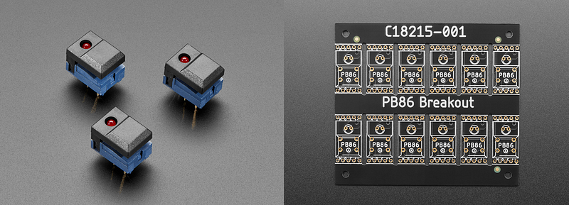
However, the switch alone doesn’t maintain the "ON" or "OFF" state I require; it functions as a momentary switch. This meant I had to devise a method for retaining the state.
Other Button Solutions
If you’re searching for alternative manufacturers, you can find various interesting options at http://www.honyone.com/en/products/list_42_1.html.
Understanding Logic Circuits
I found that the initial solution I tested utilized two NOT circuits (two gates of a NOR IC converted into NOT gates) alongside timing and capacitance quirks to create a memory cell. While it worked, it wasn't a sustainable solution, as the input relied on capacitors discharging through the switch. This energy surge could eventually damage the switch, which is not ideal for long-term use.

A More Reliable Solution: Flip-Flops
There are numerous ways to tackle this circuit, including the use of a D-Type Flip-Flop IC. While single flip-flop ICs exist, they are often part of hex (6) flip-flop packages, which may lead to unnecessary energy loss. I aim to find a single IC that can fulfill the requirement without wasting pins.
My father suggested the classic 555 timer, a versatile component capable of generating clock pulses for various applications, including toggling states and debouncing. I may eventually use a 556, which contains two 555 timers, but for now, I will test a single 555.
Let’s Explore the Circuit
I found several circuits to consider for my 555 timer project. I chose one by Bill Bowden due to his clear explanation. I plan to add a resistor/capacitor combination on pin 4 to prevent toggling upon power-up.
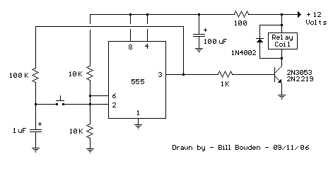
The resistors on the switch side will limit the current from the capacitor, ensuring reliable operation.
Debouncing Techniques
While discussing with my father, he mentioned the concept of a Kalman Filter for debouncing. Online research led me to several helpful articles and videos, including one from Maya’s Electronics Blog that discussed effective debouncing techniques. I believe the left side of my circuit may serve as a filter, so I will proceed with this design.
Does It Work?
In discussions on Twitter, Ahmet Inan simulated my circuit and reported promising results. Although the transition voltage may be a bit soft for older CMOS logic, it seems adequate for TTL applications.
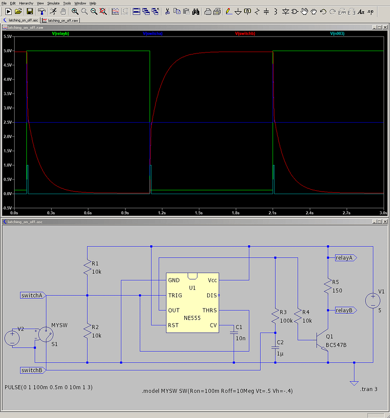
Using a Schmitt Trigger
When creating a complete array of buttons, I plan to incorporate a Schmitt trigger IC like the 74HC14, which can manage multiple switches for debouncing. For now, I will focus on a single debounce mechanism while I familiarize myself with the concept.
Prototyping the Breadboard
Here’s my work in progress, where I mark sections as "complete" using colored pencils. This method helps me track my progress and identify potential mistakes.

After completing the soldering, I ran a smoke test to check for functionality.
Improvements to Consider
Post-construction, I realized I needed to add a wire to the 555 output (Pin 3) for compatibility with digital circuits. I also overlooked a 100 Ohm current-limiting resistor. For now, it's sufficient for testing.
KiCAD/Footprint Creation
I’ll start with Adafruit’s PCB design as a foundation for my footprint experiments. Initially, KiCAD can only read schematics, so I’ll have to create the footprint manually. I found a useful KiCAD walkthrough on PCBWay.
Searching GitHub, I located a footprint for the A0 and A1, but there were discrepancies in pinouts. I managed to modify the footprint to align with my button documentation.

Final Steps in KiCAD
Here’s my schematic in KiCAD. While it may not be perfect, I’ve made significant progress.
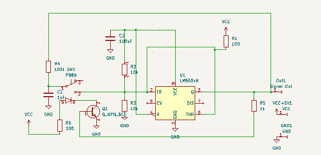
I am working on the layout to maximize space while using DIP chips. My goal is to create a compact and solder-friendly board, although my Glowforge is primarily suited for single-sided connections.
Professional PCB Production
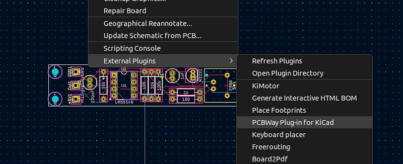
Let’s see how this design translates into an actual PCB. I’ll utilize PCBWay’s KiCAD plugin for the production process, which will allow me to learn while I navigate the integration.
- Open KiCad and access the Plugin and Content Manager.

- Search for "PCBWay" in the filter box.

- Click "Install," then "Apply Changes."
Once I clean up the PCB, I plan to send it to PCBWay using their plugin, which simplifies the ordering process.
Final Product Evaluation
The PCB arrived within a week, and I tested the PB86 footprint to ensure it fit correctly.

Despite some mistakes on my part, I soldered the components, and it looks promising. Unfortunately, it didn't function correctly, but I'm confident I can identify and rectify the issues.
Next Steps
This IC-based toggle switch meets my initial requirements. However, I aspire to create a 16-bit keyboard with additional keys. Instead of using separate 555 timers for each button, I plan to use Hex Schmitt triggers for debouncing and Hex Flip-flops to manage the inputs. This will be the focus of my next article.